I2S Receiver With A Wishbone Interface For The ZPUino
The I2S bus was introduced by Philips Semiconductor in 1986. Its purpose is to provide a simple serial interface capable of transferring digital audio data between integrated circuits so, when I needed a way to transfer data between a Teensy microcontroller and my Papilio One FPGA board, an I2S receiver was a natural choice.
I like to work with the ZPUino System-on-Chip (SoC) so I prefer FPGA blocks containing a WishBone interface. Since the I2S signal specification isn’t that complicated I decided to write one myself.
Examining the I2S Data Stream
The figure below from the I2S bus specification shows a single frame in an I2S data stream.

There are three signals, the serial clock (SD), left-right clock (WS), and serial data (SD). The serial clock and left-right clock can be generated from either the transmit or receive side. The side that generates them is called the master, the side receiving them is the slave.
For the case I’m interested in (transferring digital audio from a Teensy microcontroller to an FPGA), the clocks are generated by the Teensy so the block described here is an I2S slave receiver. Implementing it comes down to three things; clock synchronization/edge detection, left-right channel detection, and sampling the audio data.
Clock Synchronization and Edge Detection – FPGAs are synchronous devices. They like to operate on the rising edge of their clocks. Unfortunately an I2S slave receiver operates within the transmitter’s clock domain so the first thing that needs to be done is bring the I2S data stream into the FPGA clock domain.
A circuit for doing this is shown below. The first flip-flop samples the incoming data stream. There will be meta-stability problems with the signal out of the flop-flop because we’re dealing with two different clock domains and a violation of the flip-flop setup and hold time at some point is inevitable. Therefore, the output of the first flip-flop is sampled by a second flip-flop. The output of the second flip-flop puts the incoming data stream into the FPGA clock domain.
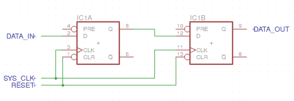
But as mentioned above, FPGAs like to operate on system clock edges. To identify the clock edges in the incoming data stream a third flip-flop is added. The clock edges are recognized by looking for differences in the output of the second and third flip-flops. VHDL code to do this for the I2S serial clock is listed below. Code for the left-right clock is similar.
    -- Process to detect the positive and negative edges of the sclk.
    -- This process syncs the sclk into the FPGA clock domain.
    -- For a description of how this works, see
    -- https://www.doulos.com/knowhow/fpga/synchronisation/
    -- These edge signals are only valid for a single system clock.
    --
    detect_sclk_edge : process(wb_rst_i, wb_clk_i)
    begin
    if wb_rst_i = '1' then
      zsclk <= '0';
      zzsclk <= '0';
      zzzsclk <= '0';
      sclk_pos_edge <= '0';
      sclk_neg_edge <= '0';
    elsif rising_edge(wb_clk_i) then
      zsclk   <= sclk_in;
      zzsclk  <= zsclk;
      zzzsclk <= zzsclk;
      if zzsclk = '1' and zzzsclk = '0' then
        sclk_pos_edge <= '1';
        sclk_neg_edge <= '0';
      elsif zzsclk = '0' and zzzsclk = '1' then
        sclk_pos_edge <= '0';
        sclk_neg_edge <= '1';
      else
        sclk_pos_edge <= '0';
        sclk_neg_edge <= '0';
      end if;
    end if;
    end process;
Left-Right Channel Detection – Once the code to locate rising and falling edges of the left-right clock is implemented, recognizing the start of the left and right channel data is as simple as looking for left-right clock falling and rising edges.
Recognizing the start of the left and right channel data is important since that’s when initialization required to sample the data for that channel is done. Examples include initialization of the channel data register, clearing the counter used to keep track of sampled data bits, etc. Once the initialization is complete you can move on to …
Sampling The Audio Data – While the left-right clock edge occurs on a falling edge of the serial clock, the serial audio data is valid and sampled on the rising edge. It begins on the second serial clock rising edge after the left-right clock edge and is sent most significant bit (MSB) first. Sampling the audio data is as simple as shifting the appropriate number of bits into registers for the left and right channels. Code to accomplish the left-right channel detection and data sampling is listed below.
    --
    -- Process to create state counter for the left-right
    -- channel.
    --
    process(wb_rst_i, wb_clk_i)
      variable left_state  : integer := 0;
      variable right_state : integer := 0;
    begin
      if wb_rst_i = '1' then
        --
        -- Initialize.
        --
        left_channel_state  <= (others => '0');
        left_channel_data   <= (others => '0');
        left_channel_reg    <= (others => '0');
        right_channel_state <= (others => '0');
        right_channel_data  <= (others => '0');
        right_channel_reg   <= (others => '0');
        sample_ready        <= '0';
      elsif rising_edge(wb_clk_i) then
        --
        -- Prepare to receive channel data on the rising/falling edge of the
        -- left/right clock.
        --
        if lrclk_neg_edge = '1' then
          --
          -- Starting the left channel so initialize and save the right channel.
          --
          left_channel_data <= (others => '0');
          left_channel_state <= (others => '0');
          case control_reg(0) is
            when '0' =>
              --
              -- I2S format.
              --
              right_channel_reg <= right_channel_data(AUDIO_DATA_WIDTH-2 downto 0) & '0';
            when '1' =>
              --
              -- Left justified.
              --
              right_channel_reg <= right_channel_data(AUDIO_DATA_WIDTH-1 downto 0);
            when others =>
          end case;
          --
          -- Having saved the right channel sample indicates the end of an audio
          -- frame.  Set the flag indicating the sample pair is ready.
          --
          sample_ready <= not(sample_read);
        elsif lrclk_pos_edge = '1' then
          --
          -- Starting the right channel so initialize and save the left channel.
          --
          right_channel_data <= (others => '0');
          right_channel_state <= (others => '0');
          case control_reg(0) is
            when '0' =>
              --
              -- I2S format.
              --
              left_channel_reg <= left_channel_data(AUDIO_DATA_WIDTH-2 downto 0) & '0';
            when '1' =>
              --
              -- Left justified.
              --
              left_channel_reg <= left_channel_data(AUDIO_DATA_WIDTH-1 downto 0);
            when others =>
          end case;
        end if;

        --
        -- Process incoming data on the rising edge of the sclk.
        --
        if sclk_pos_edge = '1' then
          --
          -- Processing for the left channel.
          --
          if left_channel_clock = '1' then
            --
            -- Update the left channel state
            --
            left_state  := to_integer(left_channel_state);
            left_channel_state <= to_unsigned(left_state + 1, CHANNEL_STATE_LENGTH);

            --
            -- Update the channel and output data.
            --
            if left_state < AUDIO_DATA_WIDTH then
              left_channel_data <= left_channel_data(AUDIO_DATA_WIDTH-2 downto 0) & audio_in;
            end if;
          else
            --
            -- Update the right channel state
            --
            right_state := to_integer(right_channel_state);
            right_channel_state <= to_unsigned(right_state + 1, CHANNEL_STATE_LENGTH);

            --
            -- Update the channel and output data.
            --
            if right_state < AUDIO_DATA_WIDTH then
              right_channel_data <= right_channel_data(AUDIO_DATA_WIDTH-2 downto 0) & audio_in;
            end if;
          end if;
        end if;
      end if;
    end process;
Using the Block
The VHDL source along with a ZPUino class for using it is available in my GitHub repository. Control and status registers for the Wishbone interface are as defined below.
| DataDirection | Address | Name | Description1 |
|---|---|---|---|
| IN | 000 | Control Bits | 0 – Left/Right Align2 |
| OUT | 000 | Status Bits | 0 – Left/Right Align current value 1 – Audio sample ready |
| 001 | Audio Sample | 31 bit sample. Upper 16 bits contain the left channel data. Lower 16 bits contain the right channel data. |
Notes: 1. Status and control bits are active high. 2. If 0 the audio data within a channel is sampled beginning on the second rising edge of the serial data clock. If 1 sampling begins on the first rising edge. |
The block was tested at 44.1 kHz but there’s nothing rate specific so it should function just fine at 48 kHz.
- Posted in: Uncategorized
- Tagged: FPGA, Papilio One, vhdl, Zpuino
